

TSMC’s 1.4nm Fab in Taichung Runs Ahead of Schedule, Mass Production Slated for Mid-2028

TLDR
- TSMC’s US$49 billion 1.4nm fab in Taichung’s Central Taiwan Science Park is running months ahead of schedule, with the first building expected before April 2027.
- First silicon could be running in April 2027 and pilot production kicks off in Q3 2027, with mass production targeted for mid-2028.
- The first two of four planned fabs are already in the steel-structure phase, with AI-powered image recognition and intelligent safety inspection deployed on site.
- TSMC’s A14 node is hitting roughly 90 percent of target transistor performance and 90 percent yield on a 256Mb SRAM test vehicle, with strong pull from smartphone and AI/HPC customers.
- For Malaysia, the Central Taiwan ramp means fresh demand for back-end test, assembly, equipment spares and tooling suppliers across Penang, Kulim and the wider northern corridor.
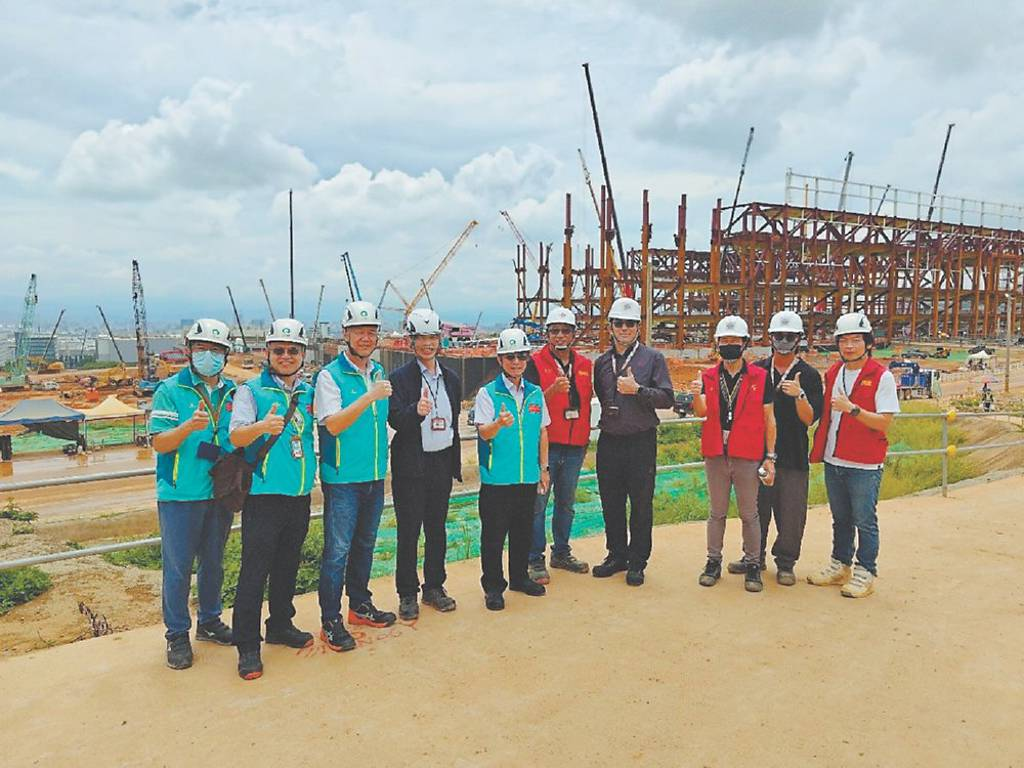
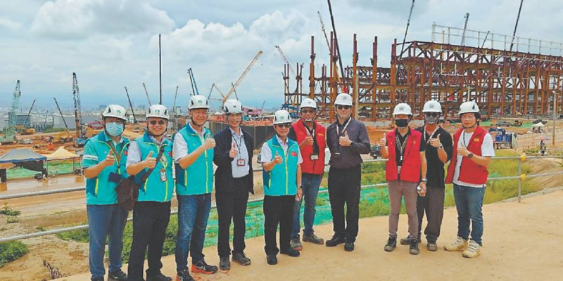
TSMC is pulling ahead in the global race to 1.4nm-class chipmaking. According to Commercial Times and confirmed by TrendForce and Electronics Weekly, construction of the foundry giant’s US$49 billion 1.4nm fab at the Central Taiwan Science Park in Taichung is running noticeably ahead of schedule, with the first building expected to wrap up before April 2027.

Central Taiwan Science Park Administration Director Hsu Mao-hsin said foundation piling is largely done and work has advanced to the central utility plant (CUP) and office buildings. Two of the four planned fabs have moved into the steel-structure phase, putting the cluster months ahead of the original timeline. If equipment installation and line qualification go smoothly, TSMC could see first silicon as early as April 2027, with a pilot run starting at the beginning of Q3 2027 and full mass production landing by mid-2028.
What’s Under the Roof
The Taichung fab will use TSMC’s second-generation gate-all-around (GAA) transistor architecture and, in a notable departure from the bleeding edge, will not rely on ASML’s latest High-NA EUV lithography machines. That decision keeps tooling costs and operational complexity more manageable while still pushing toward 1.4nm-class density and power efficiency.
During its most recent earnings call, TSMC confirmed that its A14 (1.4nm-class) process has outpaced N2 at the same development stage. Internal product-like vehicle validation is now showing transistor performance approaching 90 percent of target, with nearly 90 percent yield on a 256Mb SRAM test chip. Customer interest is described as strong across both smartphone and AI/HPC applications, the demand mix that justifies the US$49 billion price tag in the first place.
To keep construction on its accelerated track, TSMC has rolled out AI-powered image recognition and intelligent safety inspection systems on site, alongside heat-stress early warning mechanisms for crews working through Taiwan’s humid summer months. Semiconductor equipment vendors, cleanroom builders and facility engineering firms around the park are already ramping up their own investments in response.
The 1.4nm Race: TSMC vs Intel vs Samsung
The Taichung timeline puts TSMC roughly neck-and-neck with Intel in the 1.4nm window. Intel has committed to starting high-volume manufacturing on its 14A (1.4nm-class) node in 2028, with risk production of internal products slated for the second half of 2027. That aligns closely with TSMC’s mid-2028 mass production target, which means both companies will likely be shipping 1.4nm-class silicon within months of each other.
Samsung Foundry, after reportedly sliding on its original roadmap, is now targeting 1.4nm (SF1.4) mass production for 2029, putting it a full year behind the leaders. That gap matters: advanced-node lead time is one of the few moats left in the foundry business, and a year-long slip is enough to push flagship smartphone and AI accelerator designs toward whichever foundry ships first.
Our Take
The Taichung fab’s acceleration is more than a construction update. It is a strategic signal that TSMC intends to defend its advanced-node lead at a moment when AI accelerator demand is pulling forward every quarter. Hitting mid-2028 mass production means the company’s biggest customers (Apple, NVIDIA, AMD, Qualcomm, MediaTek, Broadcom) will have a clear 1.4nm-class roadmap to design against, locking in tool orders, EDA commitments and packaging capacity for the next design cycle.
For Malaysia, the ripple effect is real even though no wafer will be made here. Penang and Kulim already host the world’s largest back-end semiconductor cluster, and a faster Taichung ramp means more 2nm and 1.4nm die flowing through OSAT partners such as ASE Malaysia, Inari and Unisem, plus the broader Vitrox, Pentamaster and Mi Technovation supply chain. Equipment vendors and cleanroom specialists with TSMC qualification should expect elevated demand for spares, retrofits and new tooling lines through 2027 and 2028. If TSMC hits its mid-2028 mass production target, the Malaysian back-end ecosystem will be one of the clearest secondary beneficiaries.




[…] 📖 Baca versi English: TSMC’s 1.4nm Fab in Taichung Runs Ahead of Schedule, Mass Production Slated for Mid-2028 […]