

Cadence PCIe 6.0 Subsystem Hits First-Pass Compliance On TSMC N3, Now Available For SoC Design-In

TLDR
- Cadence has achieved first-pass PCI Express 6.0 specification compliance for its PHY and controller IP at the official PCI-SIG compliance workshop held in late July 2026
- The x8 subsystem was implemented in TSMC’s N3 process and tested at the full PCIe 6.0 specification speed of 64 GT/s
- Both PHY and controller passed all official PCIe 6.0 compliance tests in a single attempt and are on PCI-SIG’s Integrators List
- Positron AI has licensed Cadence’s SerDes IP for the PCIe 6.0 spec for an AI inference accelerator, citing the silicon-built subsystem and the interoperability testing as the reason
- The complete subsystem solution — PHY plus controller — is available now for SoC providers to design in, on the TSMC N3 process with x8 configuration
Cadence’s PCIe 6.0 Subsystem Hits First-Pass Compliance

Cadence has confirmed that its complete subsystem solution for the PCI Express 6.0 specification — PHY plus controller, built on TSMC’s N3 process — passed all official PCIe 6.0 compliance tests in a single attempt at the PCI-SIG compliance workshop held in late July 2026. The x8 configuration was tested at the full spec speed of 64 GT/s, and both the PHY and controller are now on PCI-SIG’s Integrators List.
First-pass compliance is a meaningful marker in the silicon IP world. Most subsystems take multiple workshop iterations to clear the spec, so getting it right on the first try signals both engineering maturity and close pre-workshop collaboration with test equipment vendors.
Why PCIe 6.0 Matters Right Now
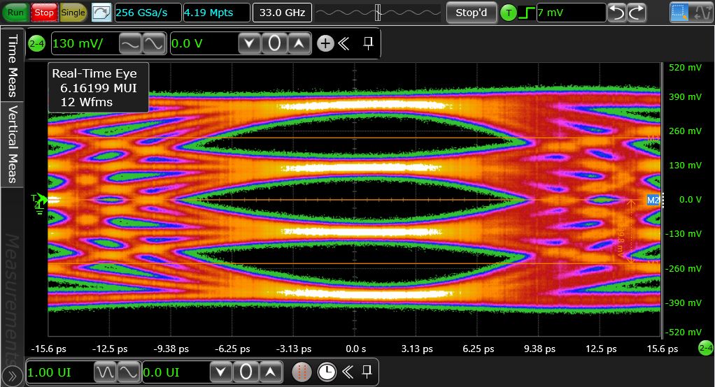
PCI Express is the scale-up interconnect that links accelerator cards, network interfaces, and storage devices inside modern AI and high-performance computing systems. The 6.0 specification doubles the per-lane bandwidth over 5.0 (to 64 GT/s) and introduces PAM4 signalling, which gives the bandwidth headroom that AI training and inference clusters need as model sizes keep growing.
For data centres and AI factories, the practical implication is that any subsystem IP failing early compliance tests creates a scheduling risk for SoC vendors trying to ship silicon on time. Cadence clearing the spec on first pass is therefore more than a PR win — it removes one of the known unknowns in an accelerator or NIC design cycle.
The Stakes For SoC Providers
Cadence’s subsystem is now available for SoC providers to design in, which means it can move from the Integrators List into real silicon designs without further compliance gating. The company is also offering the same IP family up to the PCIe 7.0 specification, giving customers a single vendor path across the current and next-generation specs.
The customer endorsement matters here. Positron AI, which is building AI inference accelerators, has licensed Cadence’s SerDes IP for PCIe 6.0 specifically because the silicon-built subsystem and the interoperability testing done before the workshop gave them the confidence to commit. For a smaller accelerator company building bleeding-edge silicon, that kind of pre-validated IP lowers design risk and shrinks time-to-market in a measurable way.
What The Subsystem Includes
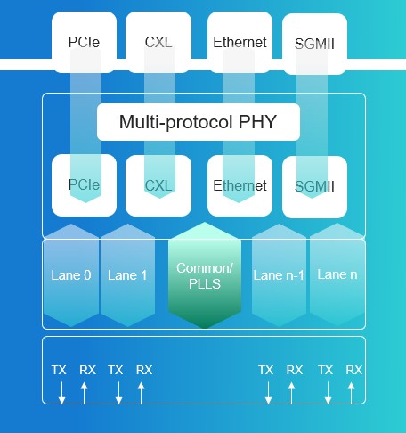
The Cadence subsystem is not just the PHY — it pairs the SerDes with a controller, firmware-tuned SerDes operation, ADC and DSP-based equalisation, and multi-protocol flexibility that covers CXL alongside PCIe. The PHY is also engineered for low power, including support for the latest PCI-SIG engineering change notices (ECNs), which keeps customers from having to redo integration as the standard matures.
For SoC teams, the practical benefit is fewer integration surprises. A subsystem that ships compliance-tested and firmware-tuned reduces the time the engineering team spends on validation, freeing them to focus on their own application logic rather than fighting PHY-level issues.
Industry Context
PCI-SIG has continued advancing the PCIe standard to keep pace with HPC and AI workloads, and the official compliance workshop is a key milestone in that cycle. Cadence’s first-pass achievement signals that the PCIe 6.0 ecosystem is moving from specification to deployment-ready silicon, which matters for hyperscale operators planning AI infrastructure rollouts over the next 12 to 24 months.
The validation work was supported by Keysight’s test and measurement solutions, which is the same instrumentation stack that hyperscale operators and accelerator vendors use for their own compliance and bring-up testing — so there is one coherent measurement chain from pre-workshop validation through to customer bring-up.
Our Take
PCIe 6.0 compliance is the kind of milestone that sounds boring until you remember how many AI accelerator timelines depend on it. Every SoC targeting AI training or inference clusters in 2027 and beyond is going to need 6.0 silicon, and the IP vendors that get there cleanly are effectively setting the clock for everyone else. Cadence’s first-pass achievement, on TSMC’s most advanced production node, with a complete subsystem (not just a PHY in isolation) is a marker that the PCIe 6.0 toolchain is production-mature. For SoC teams still in early design, this is a green light to commit to 6.0 designs on N3 without building a parallel risk-mitigation track.