
SMIC N+3 7nm Node Beats Intel 18A on Metal Pitch Without EUV — What That Means for the Global Chip Race

TLDR
- SMIC’s N+3 process hits a 32.5nm minimum metal pitch — nominally tighter than Intel’s 18A in Panther Lake (about 36nm)
- Without a single EUV layer, the Chinese foundry beats TSMC’s N6 on transistor density using DUV multi-patterning and aggressive DTCO
- Raw density gain comes at a cost: Kirin 9030 lands roughly three years behind modern flagship phones on performance and efficiency
- Intel 18A still wins overall thanks to gate-all-around transistors and backside power delivery
- Huawei is already signalling a 1.4nm-class chip by 2031, putting more pressure on the global semiconductor supply chain — including back-end players in Penang and Kulim
SMIC Beats Intel 18A on Metal Pitch — Without EUV
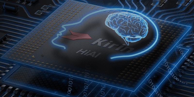
An independent teardown of Huawei’s Kirin 9030 smartphone SoC has put a number on what China’s biggest foundry can do under US sanctions. According to analysis by SemiAnalysis and partner High Yield, SMIC’s third-generation 7nm-class process — branded N+3 — supports a minimum metal pitch of 32.5 nanometres. That is nominally tighter than the roughly 36nm pitch Intel’s 18A node currently uses inside Panther Lake, even though 18A is theoretically capable of pitches down to about 32nm in some cells.
The finding lands at an awkward moment for industry roadmaps. TSMC’s N6, the long-running mobile workhorse, relies on multiple EUV layers to hit its transistor density. SMIC, cut off from ASML’s most advanced lithography, is not supposed to match that. Yet by leaning on deep-ultraviolet multi-patterning — including self-aligned quadruple patterning on the tightest layers — and aggressive design-technology co-optimisation, the Chinese foundry has reached a layout density the teardown compares favourably against TSMC’s EUV-assisted N6.
Density Without The Performance
Tighter metal pitch is not the same as a competitive node. The SemiAnalysis teardown concludes SMIC N+3 still trails Intel 18A by about 38 percent on overall transistor density, and that gap shows up where it matters most — in the products. The Kirin 9030 reportedly delivers CPU and GPU performance roughly on par with flagship application processors from three years ago, and its energy efficiency lags well behind modern Apple, Qualcomm, MediaTek and Samsung designs. Huawei’s best CPU core is broadly Cortex-X2-class in instructions-per-clock, a generation behind the Cortex-X4 and Cortex-X5 cores powering today’s top Android phones.
Intel’s 18A also pulls ahead on architecture, not just numbers on a slide. The node ships gate-all-around transistors and backside power delivery, two features that give Panther Lake a clear efficiency edge and make 18A attractive to mobile and AI accelerator designers. SMIC’s N+3 is, in SemiAnalysis’s words, a “scaled evolution” of the original 7nm that does not yet approach the architectural depth of Intel’s leading-edge logic.
Why The Malaysia Supply Chain Should Pay Attention
The geopolitical and industrial ripples reach Southeast Asia quickly. Penang and Kulim already host the world’s largest concentration of outsourced semiconductor assembly and test (OSAT) capacity, and Western chipmakers — including Intel’s advanced packaging facility in Malaysia — feed directly into the same back-end ecosystem that handles Chinese die when they clear export controls. If Huawei’s roadmap holds and SMIC pushes toward 1.4nm-class geometries by 2031, Malaysian OSATs will be evaluating new packaging, thermal management and test flows for higher-density Chinese silicon at the same time as Intel, AMD and Nvidia are pushing advanced packaging on 18A and TSMC’s N2.
The teardown also gives Malaysian policymakers a useful data point: process innovation under sanctions is slow, expensive and yields products that trail the global frontier by several years. That gap is the window in which Kuala Lumpur’s push to move up the value chain — into wafer fabrication support, advanced packaging, and design services — has to land.
Our Take
SMIC’s metal-pitch headline is a real engineering achievement, but the more important story is how uneven China’s progress still is. The foundry can squeeze density out of older DUV tools, but it cannot yet match the combination of transistor architecture, performance per watt and backside power that defines 18A and TSMC’s N2. For Malaysia, the practical takeaway is that the global semiconductor map is splitting into two tracks — a frontier track led by Intel, TSMC and Samsung, and a constrained track led by SMIC — and both will need serious back-end capacity in Penang and Kulim.
That dual-track reality makes advanced packaging a smarter national bet than chasing leading-edge fabs of our own. Malaysia should be doubling down on 2.5D and 3D packaging, chiplet integration and high-bandwidth memory test — the parts of the value chain where geopolitical positioning matters less than execution speed. SMIC catching up on metal pitch is interesting; Malaysia winning the advanced packaging race would be far more valuable.