

Rapidus and Cadence Partner on Agentic AI for Advanced Chip Design

TLDR
- Rapidus and Cadence combine Raads and InnoStack AI Super Agent for advanced-node chip design
- Target: up to 2X faster design turnaround time on SoCs built for AI infrastructure and physical AI
- Two new Rapidus tools — Raads Navigator and Raads Indicator — extend the agentic design lineup
- Integration spans architectural exploration, implementation and signoff for next-gen silicon
- Joint keynote with Rapidus CEO Atsuyoshi Koike planned at CadenceLIVE Japan 2026
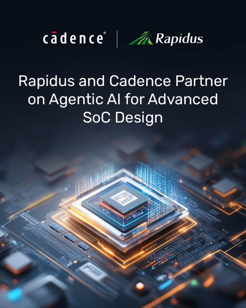
Japan’s advanced-node foundry challenger Rapidus and electronic design automation heavyweight Cadence have teamed up to push agentic AI deeper into the semiconductor design workflow. The pair will integrate Cadence’s InnoStack AI Super Agent into Rapidus’s own AI-Agentic Design Solution, branded Raads, targeting up to a two-fold acceleration in design turnaround time for advanced system-on-chips.
Rapidus Meets Cadence: An Agentic Pairing For Advanced-Node SoCs
Rapidus has spent the last few years positioning itself as a credible Western counterweight to TSMC and Samsung in leading-edge logic, with a manufacturing roadmap aimed at 2nm-class processes and below. Its Raads platform was already AI-native, but the new partnership with Cadence brings a recognised industry-standard agentic orchestration layer on top. Cadence’s InnoStack AI Super Agent is designed to coordinate multiple AI helpers across the chip design lifecycle — from early architectural exploration through implementation and signoff — so engineers can spend less time wrangling tools and more time solving design problems.
The pairing is aimed squarely at the buildout of AI infrastructure and the coming wave of “physical AI” systems — robots, autonomous platforms and edge devices that need tightly co-optimised silicon. As chip complexity spirals, the companies argue that isolated point-tool optimisations no longer cut it; orchestration across design, manufacturing and packaging is the new battleground.
Two New Tools Land In The Rapidus Stack
Alongside the Cadence tie-up, Rapidus is extending Raads with two new modules. Raads Navigator is positioned as a quality-assurance layer that helps design teams navigate complex advanced-node decisions, while Raads Indicator surfaces design issues and challenges earlier in the flow so engineers can resolve them before they metastasise. Both tools are integrated with Cadence’s agent so that design changes in one part of the stack can ripple intelligently through the rest of the flow rather than triggering cascading re-spins.
Cadence CEO Anirudh Devgan framed the deal as a step toward agentic AI becoming the connective tissue between design intent and physical silicon. Rapidus CEO Atsuyoshi Koike added that the integration is central to his company’s “Innovative Integration for Manufacturing” facility, which he described as an AI-native foundry where machine learning sits at almost every stage of production.
What This Means For The Broader Industry
For chip designers, the practical promise is shorter cycles on bleeding-edge nodes — historically the slowest, most expensive part of any silicon programme. Faster turnaround also lowers the barrier to advanced-node exploration for startups and smaller system houses that previously could not afford multiple tape-outs. For Cadence, the deal broadens the reach of its agentic AI roadmap into a foundry that is explicitly courting Western customers wary of over-concentration in Taiwan.
Our Take
The semiconductor industry loves a good “AI for AI chips” narrative, but this Rapidus-Cadence pairing has more substance than most. Raads was already built around AI-native design; adding Cadence’s agentic orchestration gives it a real chance to compress schedules on nodes where every day of tape-out slip costs real money. If the duo can hit the 2X turnaround target consistently, the ripple effect across the broader advanced-node ecosystem will be worth watching.
For Malaysia, the story is more indirect but still relevant. The country has been building out backend semiconductor capacity — packaging, testing and assembly — through players like Inari Amertron, Unisem and Globetronics, all of which stand to benefit from a healthier advanced-node design pipeline upstream. Any move that keeps more leading-edge design work flowing through Asia is good news for the regional semiconductor cluster Penang has spent a decade nurturing.
The biggest question is execution. Agentic AI in EDA is still early innings, and CadenceLIVE Japan 2026 will be the first public litmus test of how well Raads and InnoStack actually cooperate in front of real customers. Watch the keynote closely — that is where the marketing slides end and the engineering receipts begin.